 | ÐлекÑÑоннÑй компоненÑ: DM6580L | СкаÑаÑÑ:  PDF PDF  ZIP ZIP |
Äîêóìåíòàöèÿ è îïèñàíèÿ www.docs.chipfind.ru
DM562P
V.90 Integrated Data/ Fax/Voice/Speakerphone
Modem Device Single Chip with Memory Built in
Preliminary
1
Version: DM562P-DS-P02
February 28, 2001
General Description
The DM562P integrated modem is a two-chipset
design that provides a complete solution for state-
of-the-art, voice-band Plain Old Telephone
Switching (POTS) communication. The modem
provides for Data (up to 56,000bps), Fax (up to
14,400bps), Voice and Full Duplex Speaker-phone
functions to comply with various international
standards.
The design of the DM562P is optimized for desktop
personal computer applications and it provides a low
cost, highly reliable, maximum integration, with the
minimum amount of support required. The DM562P
modem can operate over a dial-up network (PSTN)
or 2 wire leased lines.
The modem integrates auto dial and answer
capabilities, asynchronous data transmissions,
serial and parallel interfaces, various tone detection
schemes and data test modes.
The DM562P modem reference design is pre-
approved for FCC part 68 and provides minimum
design cycle time, with minimum cost to insure the
maximum amount of success.
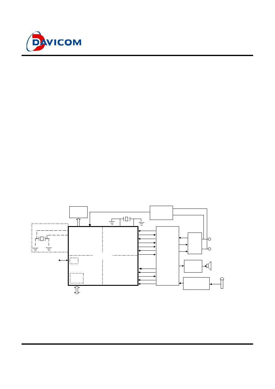
The simplified modem system, shown in figure
below, illustrates the basic interconnection between
the MCU, DSP, AFE and other basic components of
a modem. The individual elements of the DM562P
are:
·
DM6580 Analog Front End (AFE). 28-pin PLCC
package
·
DM6588 ITU-T V.90 integrated Processors with
32K bytes SRAM built in 128-pin QFP package
Block Diagram
LED
Micro
Controller
Unit
TX DSP
Ring
Detector
DM6580
Analog
Front End
SCLK
DIT
DOT
TFS
DIR
DOR
RFS
RXSCLK
CLKIN
TXDCLK
RXDCLK
DAA
RxIN
TxA1
TxA2
Line
Speaker
Driver
PCI
Bus
RX DSP
V.24
Interface
V.24
Interface
PnP
SPKR
Microphone
Driver
29.4912MHz
30.24MHz
Optional
DM6588
DM6588
DM6588
DM6588
TXSCLK*2

DM562P
V.90 Integrated Data/ Fax/Voice/Speakerphone
Modem Device Single Chip with Memory Built in
2
Preliminary
Version: DM562P-DS-P02
February 28, 2001
Features
Compatibility
-
ITU-T V.90 (56000 to 28000 bps)
- ITU-T V.34 (33600 to 2400 bps)
- CCITT V.32bis (14400, 12000, 9600,
7200, 4800bps)
-
CCITT V.32 (9600, 4800bps)
-
CCITT V.22bis (2400, 1200bps)
-
CCITT V.22 (1200bps)
-
CCITT V.23 (1200/75bps)
-
CCITT V.21 (300bps)
-
Bell 212A (1200bps)
-
Bell 103 (300bps)
Fax
-
CCITT V.17 (14400, 12000,
9600,7200bps)
-
CCITT V.29 (9600, 7200bps)
-
CCITT V.27ter (4800, 2400bps)
-
CCITT V.21 Channel 2 (300bps)
-
Group III, Class 1
Data
Error
Correction
- MNP
Class
4
-
CCITT V.42 LAPM
Data
Compression
- MNP
Class5
- CCITT
V.42bis
Voice
compression
-
2,3 and 4 bit ADPCM
- IMA
ADPCM
(Developing)
- 8
Bit
PCM
DTE
Interface
-
DTE speed up to 115200bps
Enhanced "AT" command set and S registers
-
TIA/EIA 602, ITU V.25 ter AT command
Set
-
TIA/EIA 578 Fax Class 1 command set
-
-
TIA/EIA IS-101 Voice command set
Integrated
UART
16550
Serial
interfaces
-
6, 7 and 8 bit character support
-
Even, odd, mark and none parity
detection and generation
-
1 and 2 stop bit support
-
Auto DTE data speed detection through
"AT"
Parallel
interfaces
(PCI)
- PCI Plug and Play (PnP) support
- Compliant with PCI specification 2.1
- Compliant with the Advanced
Configuration and
- ower Interface Specification(ACPI) revision
1.0
- Compliant with PCI bus Power
Management Interface Specification
revision 1.0
Caller identification (Caller ID) support
Speakerphone
Selectable world wide call progress tone
detection
Enhanced 8032 compatible micro-controller
Power
down
mode
Access up to 256K bytes external program
memory
Access up to 64K bytes external data memory
NVRAM to store two user configurable,
selectable profiles with three programmable
telephone numbers
32K bytes SRAM built in
DM562P
V.90 Integrated Data/ Fax/Voice/Speakerphone
Modem Device Single Chip with Memory Built in
Preliminary
3
Version: DM562P-DS-P02
February 28, 2001
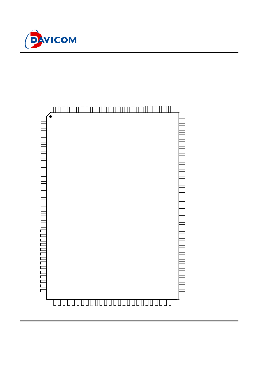
Chip 1:Integrated Processor Unit with RS232 and PNP for PCI
DM6588 External Pin Configuration
UD0
UD1
UD2
UD3
GND
RXDCLK
UD5
RD_SP2
TXDCLK
GND
DSPTXD
OUTP3
1
2
3
4
5
6
7
8
9
10
11
12
13
14
15
16
17
18
19
20
21
22
118
119
120
121
122
123
124
125
126
127
128
VD
D
DM6588
External
43
42
41
40
39
OUTP2
OUTP1
23
24
25
26
28
27
29
VDD
GND
31
32
33
34
36
38
35
37
52
51
50
48
49
47
46
45
44
58
57
56
55
54
53
64
63
62
61
60
59
115
116
117
OSC
O
OSC
I
102
101
100
99
98
97
96
94
95
93
92
91
90
89
88
87
86
85
84
83
82
81
80
79
78
77
76
75
74
73
72
71
70
69
68
67
66
65
109
110
111
112
113
114
F
R
_SP1
/PO
R
Voi
c
e Sel
1
Voi
c
e Sel
2
CO
DE
C_
CL
K
VD
D
103
104
105
106
107
108
D3
D2
D1
D0
F
R
_SP2
GN
D
UD4
VCC
UD7
UD6
GND
D4
D5
CA1
VDD
CA4
CA7
GND
CA6
CA5
CA3
CA2
CA0
D7
D6
CA9
CA10
CA11
CA12
CA13
CA14
CA15
CA8
RD_SP1
OUTP0
INP2
INP3
INP0
INP1
DSPRXD
T
EST
1
RESET
TEST2
TEST3
30
TXSCLK
GND_AUX
/R
I
EEPR
OM
3
EEPR
OM
2
EEPR
OM
1
/VO
I
C
E
/D
T
R
/O
H
XT
AL2
XT
AL1
CA
1
7
/PWR
VD
D
T1
T0
GN
D
CA
1
6
T
D
_SP1
/RD
/WR
/PSEN
TXD
RXD
VDD
/LCS
RXSCLK
VCC_AUX
GN
D
SCLK
T
D
_SP2
EXT
/IN
B
GN
D
PS1
TEST4
DM562P
V.90 Integrated Data/ Fax/Voice/Speakerphone
Modem Device Single Chip with Memory Built in
4
Preliminary
Version: DM562P-DS-P02
February 28, 2001
AD27
AD26
AD25
AD24
GND
IDSEL
C/BE3#
AD22
AD16
C/BE2#
FRAME#
GND
IRDY#
TRDY#
1
2
3
4
5
6
7
8
9
10
11
12
13
14
15
16
17
18
19
20
21
22
118
119
120
121
122
123
124
125
126
127
128
AD
2
8
VD
D
DM6588
PCI
AD
3
1
AD
3
0
AD
2
9
43
42
41
40
39
DEVSEL#
STOP#
23
24
25
26
28
27
29
VDD
GND
31
32
33
34
36
38
35
37
52
51
50
48
49
47
46
45
44
58
57
56
55
54
53
64
63
62
61
60
59
115
116
117
OS
C
O
OS
C
I
102
101
100
99
98
97
96
94
95
93
92
91
90
89
88
87
86
85
84
83
82
81
80
79
78
77
76
75
74
73
72
71
70
69
68
67
66
65
109
110
111
112
113
114
F
R
_
SP1
/P
OR
Vo
i
c
e
Se
l
1
Vo
i
c
e
Se
l
2
CO
DE
C_CLK
VD
D
103
104
105
106
107
108
D3
D2
D1
D0
F
R
_
SP2
GN
D
AD23
AD17
AD18
AD19
VCC
AD20
AD21
GND
AD
1
D4
D5
CA1
VDD
CA4
CA7
GND
CA6
CA5
CA3
CA2
CA0
D7
D6
CA9
CA10
CA11
CA12
CA13
CA14
CA15
CA8
C/BE1#
PAR
SERR#
PERR#
AD14
AD15
AD12
AD13
AD11
POWEROFF
T
EST
1
RST#
TEST2
TEST3
30
RIN
GND_AUX
T
XSC
L
K
EEPR
O
M
3
EEPR
O
M
2
EEPR
O
M
1
/V
OIC
E
/D
TR
/OH
XT
AL
2
XT
AL
1
AD
1
0
AD
8
AD
9
CA
17
/P
WR
VD
D
C
/
BE0
#
AD
6
AD
7
GN
D
CA
16
T
D
_
SP1
AD
4
AD
5
AD
2
AD
3
/RD
/WR
/PSEN
RD_SP1
RD_SP2
VDD
SCLK
AD0
RXSCLK
VCC_AUX
PME#
GN
D
PCLK
T
D
_
SP2
EXT
/
I
N
B
GN
D
PS1
IN
T#
TEST4
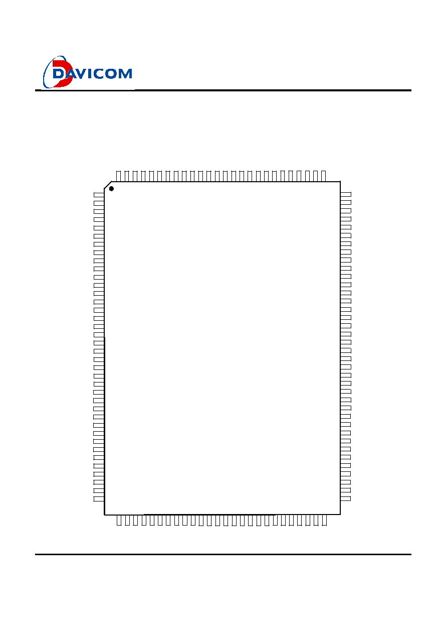
DM6588 PCI Pin Configuration
DM562P
V.90 Integrated Data/ Fax/Voice/Speakerphone
Modem Device Single Chip with Memory Built in
Preliminary
5
Version: DM562P-DS-P02
February 28, 2001
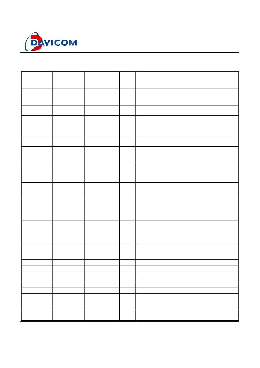
DM6588 Pin Description
Pin No.
PCI internal
Pin No.
External
Pin Name
I/O
Description
1
1
Test4
I
Test pin 4
2~5,
9~12
UD0 - UD7
O
Modem Control Output, for external modem:
Memory address mapping of the controller is
E800H.
8
RxDCLK
I
Receive Data Rate Clock:(External)
This pin is used as reference clock of DSPRXD pin.
18
RD_SP2
I
Data Input Pin Of The Serial Port 2 (External)
The serial data is sampled at the falling edge of the
SCLK. The MSB is coming immediately after the
falling of FR_SP2 signal.
19
TXDCLK
I
Transmit Data Rate Clock:(External)
This pin is used as reference clock of DSPTXD pin.
21
DSPTxD
I
Modem Transmit Data (External)
Shifted into DM6581/DM6582 from EIA port
through this pin at the rising edge of TXDCLK.
28
RD_SP1
I
Data Input Pin Of The Serial Port 1 (External)
The serial data is sampled at the falling edge of the
SCLK. The MSB is coming immediately after the
falling of FR_SP1 signal.
6,20,37
50,80,89
107,118,123
6,20,37
50,80,89
107,118,123
GND
P
Ground
22~25
OUTP3~
OUTP0
O
Modem Control Output
For external modem, these pins are bit7~4 of the
modem control output. Memory address mapping
of the controller is C800H.
29~32
INP3~INP0
I
Modem Control Input
For external modem, these pins are bit3~0 of the
modem control input. Memory address mapping of
the controller is C800H.
13,33,45
67,94,113
128
13,33,45
67,94,113
128
VDD
P
+3.3V Power Supply
34
34
TEST2
I
Test pin 2,normal ground
35
35
TEST3
I
Test pin 3,normal ground
36
RESET
I
Reset:
An active high signal used to reset the DM6588.
42
42
XTAL1
I
Crystal Oscillator Input
43
43
XTAL2
O
Crystal Oscillator Output
46
46
/PWR
O
Controller Program Write Enable:
This pin is used to enable FLASH ROM
programming.
48
48
TD_SP1
O
Data Output Pin Of Serial Port 1
The serial data is clocked out through this pin